" width="211.99999530565634px"><path d="M 0 0 L 21.672 0 L 21.672 1.445 L 0 1.445 Z M 27.452 0 L 49.124 0 L 49.124 1.445 L 27.452 1.445 Z M 54.903 0 L 76.576 0 L 76.576 1.445 L 54.903 1.445 Z M 54.903 10.114 L 76.576 10.114 L 76.576 11.558 L 54.903 11.558 Z M 27.452 20.228 L 39.01 20.228 L 39.01 21.672 L 27.452 21.672 Z M 59.238 20.228 L 72.241 20.228 L 72.241 21.672 L 59.238 21.672 Z M 39.01 10.114 L 39.01 20.227 L 37.566 20.227 L 37.566 10.114 Z" fill="rgb(26, 26, 26)" height="21.672358586906324px" id="gK_Mh2pDw" width="76.57578110701563px"/><path d="M 20.228 10.113 L 10.114 10.113 L 10.114 8.669 L 20.228 8.669 Z M 21.672 20.227 L 15.171 20.227 L 15.171 18.783 L 21.672 18.783 Z M 0 18.783 L 0 0 L 1.445 0 L 1.445 18.783 Z M 20.228 18.783 L 20.228 0 L 21.672 0 L 21.672 18.783 Z" fill="rgb(26, 26, 26)" height="20.227311744808098px" id="nN12tbtQP" transform="translate(27.507 1.5)" width="21.672358586906363px"/><path d="M 42.622 18.783 L 42.622 0 L 44.067 0 L 44.067 18.783 Z M 54.903 8.669 L 54.903 0 L 56.348 0 L 56.348 8.669 Z M 75.131 8.669 L 75.131 0 L 76.575 0 L 76.575 8.669 Z M 70.796 18.783 L 70.796 10.114 L 72.241 10.114 L 72.241 18.783 Z M 59.238 18.783 L 59.238 10.114 L 60.683 10.114 L 60.683 18.783 Z M 1.445 0 L 1.445 20.228 L 0 20.228 L 0 0 Z M 11.559 20.228 L 1.445 20.228 L 1.445 18.783 L 11.559 18.783 Z M 21.672 10.114 L 10.114 10.114 L 10.114 8.669 L 21.672 8.669 Z" fill="rgb(26, 26, 26)" height="20.227645530818847px" id="X8QQTyDlD" transform="translate(0 1.5)" width="76.57544238817589px"/><path d="M 10.114 8.958 L 10.114 0 L 11.559 0 L 11.559 8.958 Z M 0 19.072 L 0 10.403 L 1.445 10.403 L 1.445 19.072 Z M 10.114 20.517 L 10.114 13.292 L 11.559 13.292 L 11.559 20.517 Z M 4.334 20.517 L 4.334 13.292 L 5.779 13.292 L 5.779 20.517 Z M 5.78 13.292 L 10.114 13.292 L 10.114 14.737 L 5.78 14.737 Z M 5.78 19.072 L 10.114 19.072 L 10.114 20.517 L 5.78 20.517 Z M 79.032 2.456 L 92.036 2.456 L 92.036 3.901 L 79.032 3.901 Z M 96.37 2.456 L 109.373 2.456 L 109.373 3.901 L 96.37 3.901 Z M 113.708 2.456 L 126.711 2.456 L 126.711 3.901 L 113.708 3.901 Z M 135.38 2.456 L 148.384 2.456 L 148.384 3.901 L 135.38 3.901 Z M 86.256 8.236 L 92.035 8.236 L 92.035 9.681 L 86.256 9.681 Z M 97.815 8.236 L 110.818 8.236 L 110.818 9.681 L 97.815 9.681 Z M 80.477 15.46 L 93.48 15.46 L 93.48 16.904 L 80.477 16.904 Z M 97.815 15.46 L 110.818 15.46 L 110.818 16.904 L 97.815 16.904 Z M 79.032 15.46 L 79.032 3.901 L 80.477 3.901 L 80.477 15.46 Z M 96.37 15.46 L 96.37 3.901 L 97.815 3.901 L 97.815 15.46 Z M 113.708 16.905 L 113.708 3.901 L 115.153 3.901 L 115.153 16.905 Z M 135.38 15.46 L 135.38 3.901 L 136.825 3.901 L 136.825 15.46 Z M 152.718 15.46 L 152.718 2.456 L 154.163 2.456 L 154.163 15.46 Z M 170.056 15.46 L 170.056 2.456 L 171.5 2.456 L 171.5 15.46 Z M 187.394 15.46 L 187.394 2.456 L 188.839 2.456 L 188.839 15.46 Z" fill="rgb(26, 26, 26)" height="20.51672236573591px" id="FK6xE1Vot" transform="translate(10.169 1.167)" width="188.838611199974px"/><path d="M 62.127 5.78 L 75.131 5.78 L 75.131 7.224 L 62.127 7.224 Z M 79.465 5.78 L 92.469 5.78 L 92.469 7.224 L 79.465 7.224 Z M 96.803 5.78 L 108.362 5.78 L 108.362 7.224 L 96.803 7.224 Z M 79.465 0 L 91.024 0 L 91.024 1.445 L 79.465 1.445 Z M 92.469 1.445 L 92.469 5.78 L 91.024 5.78 L 91.024 1.445 Z M 109.806 7.224 L 109.806 14.448 L 108.362 14.448 L 108.362 7.224 Z M 62.127 13.003 L 75.131 13.003 L 75.131 14.448 L 62.127 14.448 Z M 79.465 13.003 L 92.469 13.003 L 92.469 14.448 L 79.465 14.448 Z M 34.675 14.448 L 34.675 1.445 L 36.12 1.445 L 36.12 14.448 Z M 56.348 13.003 L 56.348 1.445 L 57.793 1.445 L 57.793 13.003 Z M 44.789 13.003 L 57.793 13.003 L 57.793 14.448 L 44.789 14.448 Z M 39.01 14.448 L 39.01 2.89 L 40.455 2.89 L 40.455 14.448 Z M 39.01 1.445 L 39.01 0 L 40.455 0 L 40.455 1.445 Z M 0 13.003 L 0 5.779 L 1.445 5.779 L 1.445 13.003 Z M 17.338 5.78 L 17.338 1.445 L 18.782 1.445 L 18.782 5.78 Z M 106.917 0 L 108.361 0 L 108.361 1.445 L 106.917 1.445 Z M 105.472 1.445 L 106.917 1.445 L 106.917 2.89 L 105.472 2.89 Z M 104.027 2.89 L 105.472 2.89 L 105.472 4.334 L 104.027 4.334 Z M 102.583 4.334 L 104.027 4.334 L 104.027 5.779 L 102.583 5.779 Z" fill="rgb(26, 26, 26)" height="14.448460816632046px" id="P87EDhxsn" transform="translate(102.193 3.668)" width="109.80649478685751px"/></g></svg>)
A project case study showing how a playful wireless charger concept moved through product development, supplier coordination, and manufacturing preparation in Dongguan.
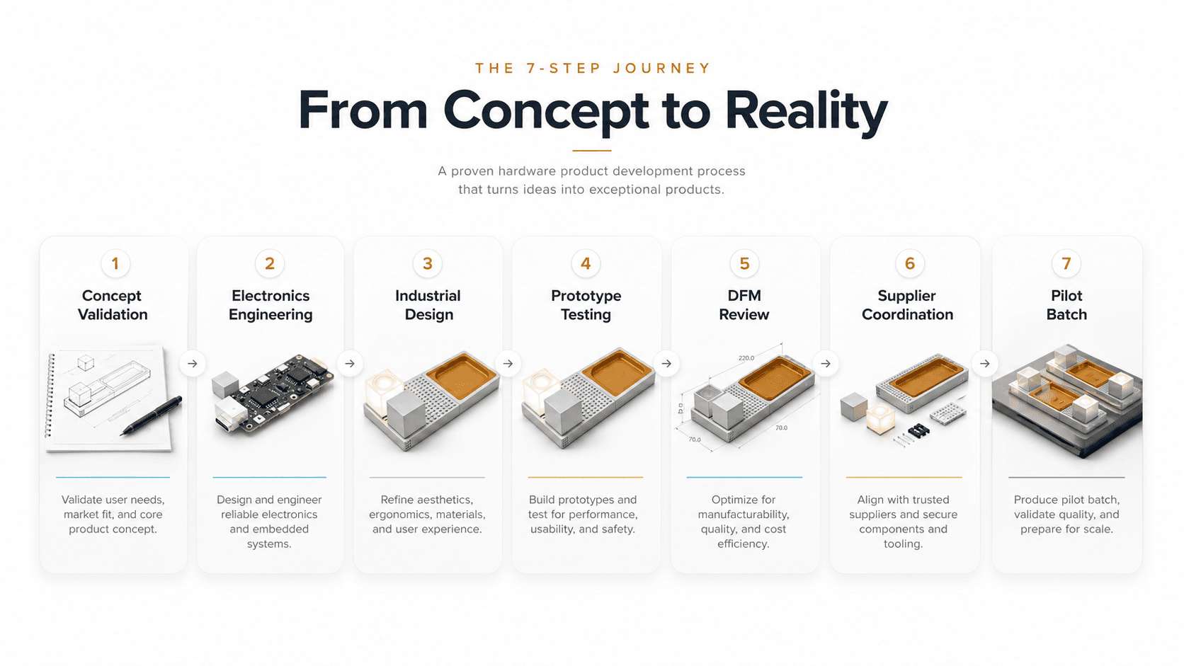
A consumer electronics founder approached GridsLab with a deceptively simple idea: a wireless charger that snapped together like Lego bricks, letting users configure their charging setup on the fly. What followed was a full wireless charger product development cycle — concept validation, electronics engineering, industrial design, and supplier coordination through Dongguan's dense manufacturing ecosystem. The project exposed every tension that hardware startups face: keeping the user experience playful while hitting cost targets, making snap-fit tolerances tight enough to be satisfying without breaking the charging coil alignment. This case study walks through how those problems got solved, and what other consumer electronics founders can take from it.
There's a category of product idea that sounds simple until you actually try to build it. A Lego-style wireless charger is exactly that kind of idea. The brief, when it first came in, was almost disarmingly offhand: modular tiles, each housing a wireless charging coil, that users could clip together into whatever shape their desk demanded. One tile for a phone. Two for a phone and earbuds. Clip on a third and charge a watch. The concept had genuine pull — modular consumer electronics is a space that Foundr and others have been watching as a real shift in how younger buyers think about ownership and customisation. But between the sketch on a napkin and a shippable product, there were probably thirty distinct engineering problems waiting to be uncovered.
GridsLab found most of them.
Why This Product Idea Was Harder Than It Looked
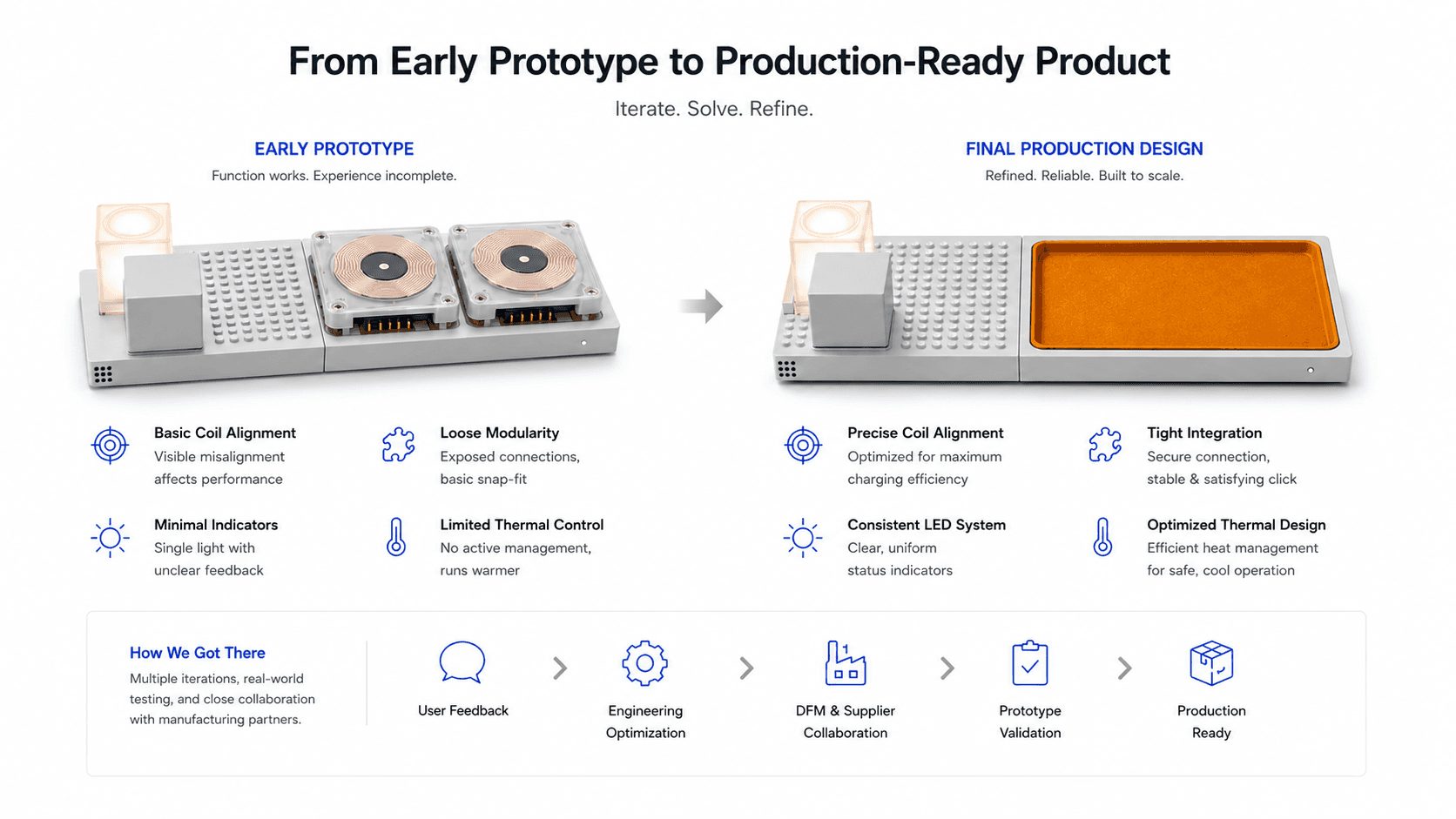
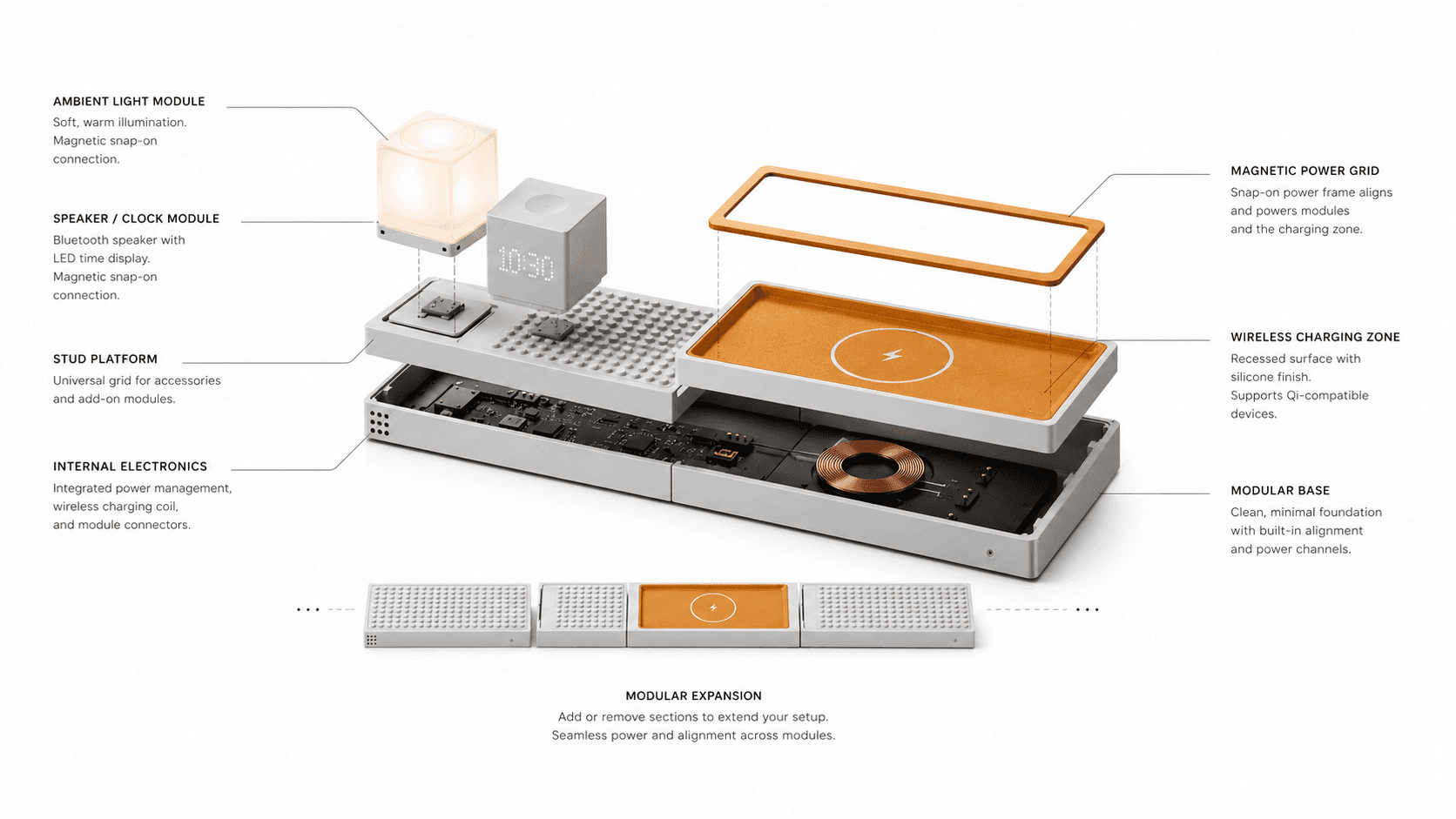
The first engineering review — which landed on a Tuesday morning, roughly three weeks into the engagement — brought the core tension to the surface immediately. Wireless charging coils are not especially forgiving of misalignment. Move a phone even a few millimetres off-axis from the coil and charging efficiency drops fast, sometimes to the point where the device simply stops charging altogether. In a fixed charger, that's handled through careful industrial design: a recessed well, a magnetic alignment ring, a precisely positioned coil. In a modular system where the tile arrangement can change at will, you lose most of those guardrails.
The snap-fit mechanism made everything harder. Lego connections feel satisfying because they're tight — there's a tactile click, a small amount of deliberate friction, and the pieces hold. Getting that same feeling in a consumer electronics context meant tolerances around 0.1mm, which is achievable in injection-moulded plastic but demands tooling investment and DFM attention that first-time founders routinely underestimate. Get the snap too loose and the tiles wobble, coils drift, charging fails. Too tight, and users can't reconfigure without feeling like they're about to snap something off.

The Electronics Side of the Problem
Underneath the mechanical challenge sat a power distribution puzzle. Each tile needed to draw power from somewhere and pass it along to adjacent tiles — otherwise users would have to plug each tile in separately, which kills the whole modular premise (which is wild, honestly, because it was the premise). This meant designing a bus system through the connectors, stepping down to safe voltages at each tile, and managing the Qi charging protocol across multiple coils that might or might not be active depending on how the user had arranged things that morning.
Not exotic engineering, exactly. But it's the kind of work that adds three weeks to a timeline and maybe $4 or $5 per unit to BOM cost if it isn't thought through carefully at the schematic stage. The team spent a meaningful stretch of the early design phase simply working out how to keep connector current-carrying capacity high enough without making the connectors themselves physically imposing.
Prototype, Refinement, and the Feedback Loop That Actually Worked
Early prototypes were — well, they were instructive. The first functional mock-up used off-the-shelf Qi modules and 3D-printed shells with hand-fit brass inserts for the connectors. It charged phones. It also ran warm enough that you wouldn't want to leave your hand on it for long, the snap-fit had about 0.4mm of play (too much), and the LED status indicators on each tile landed in slightly different positions because tolerance stack-up in the prints made exact registration impossible.
None of that is unusual for a first functional prototype. What mattered was having something physical enough to make real decisions from.
Over three or four iteration rounds — roughly eleven months of total project time saw about forty percent of it spent right here — the team worked down through the problems in roughly priority order. Thermal management first, because that was a safety concern. Coil alignment second, because it was the core product promise. Snap-fit geometry third, because it touched both the UX and the alignment problem at once. The LED placement was honestly the last thing anyone worried about — which, come to think of it, is usually how it goes.
When DFM Conversations Started Changing the Design
Design for manufacturing reviews have a way of surfacing constraints that prototype work simply doesn't reveal. The draft angles on the tile housings were initially too shallow for clean ejection at production speeds. The connector pin layout, optimised for electrical performance, created a moulding geometry that a toolmaker in Dongguan flagged as likely to produce sink marks on the visible face. Small things — but exactly the kind of small things that cost real money to fix once steel has been cut.
Getting those conversations early, ideally before the tool design is locked, is one of the structural advantages of working close to the manufacturing base.
How Dongguan's Supply Chain Shortened the Feedback Loop
Dongguan sits at the centre of a very dense web of component suppliers, toolmakers, PCB fabs, and assembly houses. That density is the whole point. For this project, it meant that when the revised connector geometry needed a new round of test pins, the lead time was days rather than weeks. When the team wanted to assess three different snap-fit geometries at once, getting three small prototype tools made and tested took about two weeks — the kind of timeline that in other manufacturing regions might stretch to six or eight.
This is what the phrase "Dongguan manufacturing case study" usually gestures at: not just cost, but speed of iteration. The cost advantage is real, but for a hardware startup, being able to run three experiments in the time it would take elsewhere to run one is often worth more than the unit economics at that stage.
Supplier Matching and Component Availability
The Qi charging modules, the bus connectors, the LED drivers, the overmoulded cables — most of these had local supplier options within a short drive of the factory floor. That matters more than it sounds. When a component is available domestically in China, lead times compress, minimum order quantities come down, and the supplier relationship is easier to manage for quality feedback. For the bus connectors specifically, the team worked with two local connector houses before settling on one whose tolerance control matched what the design actually needed.
Finding those suppliers, qualifying them, building the relationships — that's coordination work that quietly devours founder time and derails timelines for teams trying to manage it remotely. Having it handled through a hardware development partner with existing supplier relationships in the region — through hardware development services built around this kind of local coordination — compounds as an advantage across the whole project.
What the Project Proved and What Founders Can Take From It
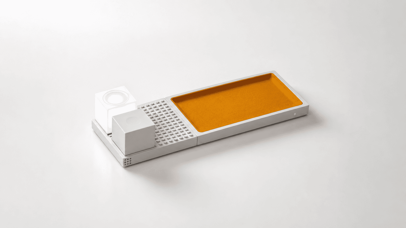
The GridsLab Lego wireless charger landed in a good place. The final design supported up to four tiles in a linear configuration, each independently capable of charging a Qi-compatible device, with a single USB-C input managing power distribution across the whole assembly. Snap-fit tolerances came in at 0.12mm in production — tight enough for the tactile click, forgiving enough that users could reconfigure without applying worrying force. Thermal performance in a four-tile configuration held within comfortable limits at 25°C ambient.
It shipped to a pilot batch. Not massive volume, but enough to validate the manufacturing process and surface any production-line issues before a larger run committed.
Worth pulling out of all this, for anyone building in consumer electronics: the problems that nearly derailed this project were all predictable. Coil alignment in a modular system. Connector current capacity. Tolerance stack-up in snap-fit geometry. None of these caught experienced hardware engineers off guard — but they did catch the founder off guard, someone who came from a software background and had genuinely underestimated how physically constrained electronics product development turns out to be.
Getting that expertise early — not after the first prototype fails thermal testing, but before the schematic is finalised — changes the trajectory entirely. It compresses the iteration cycle. The DFM conversation happens before steel is cut rather than after. And when the product finally reaches the manufacturing floor, it's actually ready.
To see the range of work this kind of process produces, the hardware product development case studies on the Geniotek site cover several different product categories at different stages of development. The patterns across them are more consistent than you'd expect. The problems change. The process that surfaces and solves them doesn't—
If you're in early-stage wireless charger product development, or working through a similar consumer electronics concept that you're not sure how to carry from sketch to factory — talk to a hardware development partner before the problems find you.